Business:
1/1

Boron (B) sputtering targets, Purity: 99.9%, CAS ID: 7440-42-8
USD $200.00 / piece
1piece (MOQ)
- FOB Price:
- Negotiable | Get Latest Price
- Order Quantity:
- 1 Set / Sets
- Supply Ability:
- 1000 Set / Sets per Month
- Port:
- shanghai
- Payment Terms:
- T/T L/C D/P D/A Credit Card PayPal Cash Escrow Other
- Delivery Detail:
- 5 days
TYR TECH MATERIAL LIMITED
Hot in store
-
Iron oxide (Fe3O4, Fe2O3) targets use in
$200.00 -

Antimony trisulfide Sb2S3 granules use i
$2000.00 -

Zirconium selenide ZrSe2 sputtering targ
$350.00 -

Yttria-stabilized zirconia Y2O3-ZrO2 YSZ
$200.00 -
Zinc Telluride ZnTe sputtering targets u
$200.00 -

Tin (Sn) metal sputtering target, purity
$100.00 -

Tungsten carbide WC targets use in RF sp
$100.00 -
Lead selenide PbSe granules use in thin
$200.00
Product Details
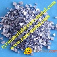
Boron (B) amorphous, CAS ID: 7440-42-8 product list from TYR as following:
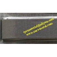
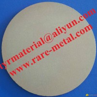
Boron, B Sputtering targets:
purity: 99.9%
Size: max. 355.6mm (14 inch) , Length: 250mm x Width 200mm x thickness 20mm max.,
Shape: Discs, disks, step disk, delta, plate, sheets or made per drawing
The melting point of boron is 2079oC, its boiling point is at 4000oC, the specific gravity of crystalline boron is 2.34g/cm3, the specific gravity of the amorphous form is 2.37g/cm3, Crystalline boron is hard, brittle, lustrous black semimetal. Amorphous boron is a brown powder.
Boron is a non-metallic element and the only non-metal of the group 13 of the periodic table the elements. The Boron are borderline between metals and non-metals (semimetallic). It is a semiconductor rather than a metallic conductor. Chemically it is closer to silicon than to aluminium, gallium, indium, and thallium.
At standard temperatures boron is a poor electrical conductor but is a good conductor at high temperatures.
Applications:
1. Glass and ceramics
2. Detergent formulations and bleaching agents
3. Semiconductors, Boron are a useful dopant for such semiconductors as silicon, germanium, and silicon carbide. Having one fewer valence electron than the host atom, it donates a hole resulting in p-type conductivity. Traditional method of introducing boron into semiconductors is via its atomic diffusion at high temperatures.
4. Magnets
5. High-hardness and abrasive compounds
6. Amorphous boron is used as a melting point depressant in nickel-chromium braze alloys.
Hexagonal boron nitride forms atomically thin layers, which have been used to enhance the electron mobility in grapheme devices. It also forms nanotubular structures (BNNTs), which have with high strength, high chemical stability, and high thermal conductivity, among its list of desirable properties
We also supply below material:
Material Name | Formula | Purity |
| Aluminum | Al | 99.99%, 99.999% |
| Antimony | Sb | 99.99%, 99.999% |
| Boron | B | 99.9%,99.99%, 99.999% |
| Barium | Ba | 99.3%, 99.9%, 99.95% |
| Bismuth | Bi | 99.99%, 99.999% |
| Graphite | C | 99.99% |
| Cobalt | Co | 99.9%, 99.95%, 99.99% |
| Chromium | Cr | 99.5%, 99.9%, 99.95% |
| Copper | Cu | 99.99%, 99.999% |
| Cadmium | Cd | 99.99% |
| Iron | Fe | 99.9%, 99.99% |
| Indium | In | 99.9%, 99.99%,99.999% |
| Lithium | Li | 99.5% |
| Molybdenum | Mo | 99.95% |
| Magnesium | Mg | 99.95% |
| Nickel | Ni | 99.9%, 99.98%, 99.995%, 99.999% |
| Niobium | Nb | 99.95% |
| Lead | Pb | 99.99% |
| Rhenium | Re | 99.95%, 99.99% |
| Silicon | Si | 99.999%, 99.9999%,poly or mono crystal, doped or undoped |
| Selenium | Se | 99.99%, 99.999% |
| Tellurium | Te | 99.99%,99.999% |
| Tantalum | Ta | 99.95%, 99.99% |
| Titanium | Ti | 99.7%, 99.99%, 99.995%, 99.999% |
| Tin | Sn | 99.99%, 99.999% |
| Tungsten | W | 99.95% |
| Vanadium | V | 99.9% |
Recommend product
-
SODIUM CARBONATE LIGHT
$300.00 -

API 2H Grade 50 Offsho
Inquiry -

Activated Carbon for P
Inquiry -
Silk protein extract p
$50.00 -
Instant pearl extract
$50.00 -
sell dyed black boiled
Inquiry -

sell horse hair horse
Inquiry -
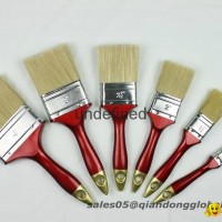
sell bristle mix filam
$3.50 -
Best Quality Chungking
$1.20 -
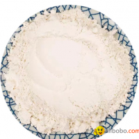
Pearl powder
Inquiry -
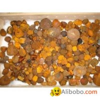
CATTLE OX GALLSTONE
$35.00 -
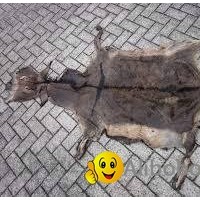
dry Donkey hides
$11.00 -

Antarctic krill oil wi
Inquiry -
horse mane and horseta
$10.76 -
feed barley
$140.00 -
animal fine hair
$10.00 -

hing qulity of the ho
Inquiry -
Animal Fine Hair
$1.00 -

Bow Hair
$5.00 -

aniaml fine hair
$1.00
Product parameters
- brand:
- TYR
closure
This shop is operated by agent
- Set up shop
- Authorized by Alibobo.com, can provide agency service
- Service Introduction
- Authorized product, Internet cloud promotion service integrating certification promotion and procurement inquiry
- Intelligent website construction
- PC terminal + mobile terminal, create a cost-effective corporate website!
closure